

Nvidia outlines AI-defined model for chip fabrication
Wed, 18th Nov 2026 (Today)
Nvidia has outlined what it calls an AI-defined model for semiconductor fabrication, combining accelerated computing, physics-based AI, AI agents and digital twins.
The model focuses on using AI tools to shorten engineering analysis in chip manufacturing, where assessing process changes, materials interactions and defects can take days, and physical experiments on production lines are costly.
Semiconductor manufacturers are under pressure as demand for advanced chips rises and manufacturing processes grow more complex. In that environment, even small errors in yield or process quality can have significant commercial consequences.
Faster simulation
A central part of the approach is faster simulation. Accelerated computing lets engineers test more alternatives before deciding which changes to try in physical production.
One of the main use cases is multiphysics simulation, which models interactions such as heat transfer, electrical behaviour and mechanical stress. Software provider COMSOL is using Nvidia's cuDSS library to speed up semiconductor manufacturing simulations by up to 10 times.
Applied Materials is also working with Nvidia on atomic-scale materials discovery and process development. Nvidia says Applied's Ginestra simulation platform runs up to 10 times faster than CPU-only approaches when integrated with cuDSS, while its ACE+ multiphysics platform delivers topography simulations up to 35 times faster with Nvidia PhysicsNeMo.
Some workloads have been difficult to run at production scale on conventional processors. Computational lithography, which determines how circuit patterns are printed onto silicon, is one example because the calculations are highly intensive.
Siemens is integrating Nvidia cuLitho into its Calibre lithography software. Nvidia says this delivers up to 17 times acceleration on key simulation workloads, giving engineers more scope to verify designs before a wafer reaches print.
Physics-based AI
Nvidia also made the case for physics-based AI models that predict how materials and manufacturing processes will behave without running a full simulation each time. It argues the benefit is greatest for expensive calculations that remain demanding even on accelerated hardware.
Plasma modelling is one example. Plasma is used in semiconductor etch processes, and modelling its behaviour requires equations that capture interactions between electrical, chemical and thermal effects.
According to Nvidia, Lam Research has shown that the Nvidia PhysicsNeMo framework can predict plasma behaviour in milliseconds, compared with days for a full simulation. That gives engineers a faster way to explore process conditions without rerunning the complete model each time.
AI agents
Nvidia also highlighted AI agents as a way to automate sequences of engineering tasks traditionally handled manually. Engineers still make the decisions in semiconductor production, but many intermediate steps can consume hours.
One example is selecting which AI model to apply to a particular task. Nvidia says Advantest is using Nvidia NeMo Switchyard AI agents to automate that process and cut response times from hours to minutes.
Digital twins
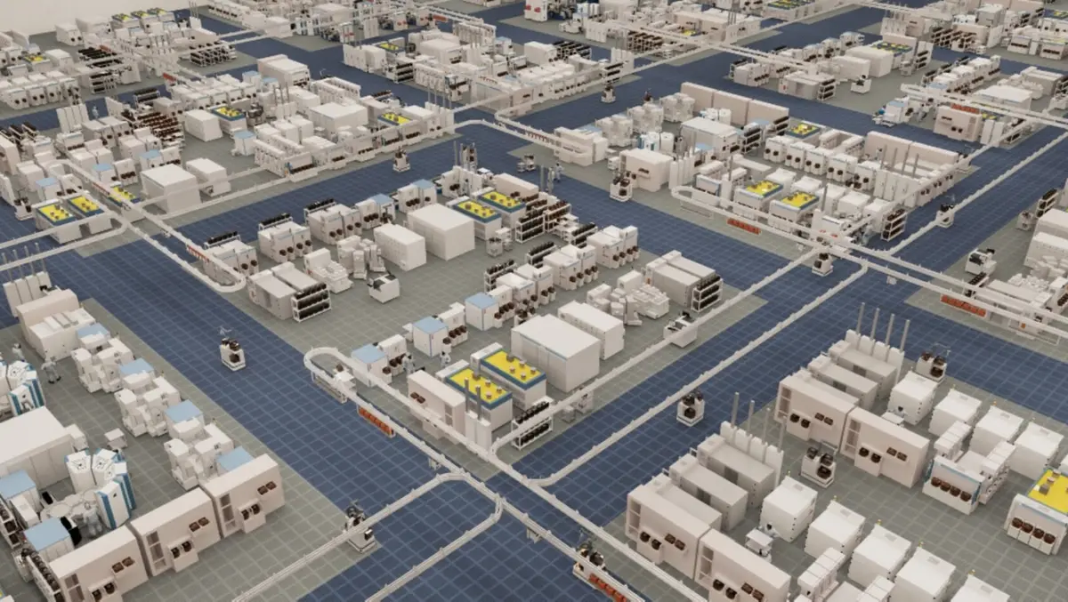
Digital twins form another part of the proposed manufacturing model. These virtual environments let teams test equipment configurations, fab layouts and process changes before carrying them out on the production line.
Applied Materials uses Nvidia Omniverse libraries to build physically accurate digital twins of entire fabrication plants, according to Nvidia. The models are used to simulate material movement, identify bottlenecks and assess layouts, throughput, cost and process control.
The aim is to extend simulation beyond individual manufacturing steps to the operation of the factory as a whole. That is increasingly relevant as fabrication plants become more complex and the cost of unsuccessful process changes rises.
Connected workflow
Nvidia's broader argument is that these technologies become more useful when linked in a closed engineering loop. In that model, production data informs simulations and AI models, which are then used to test alternatives before engineers make decisions on the factory floor.
Nvidia presented this as a way to shorten feedback cycles across semiconductor manufacturing. The aim, it says, is to help engineers identify problems earlier, evaluate more options and act on production insights sooner.
The push comes as chipmakers and their suppliers look for ways to manage greater process complexity without relying solely on slower, more expensive physical trials.